
802.11b中采用7位移位寄存器作为加扰及解扰的主题移位寄存器,加扰和解扰是自同步的乘性加扰和解扰。其生成多项式为G(X)=X7 + X4 +1,根据上节内容可以画出乘性加扰及解扰的LFSR (Linear Feedback Shift Register)时序逻辑图,如图1和图2所示。
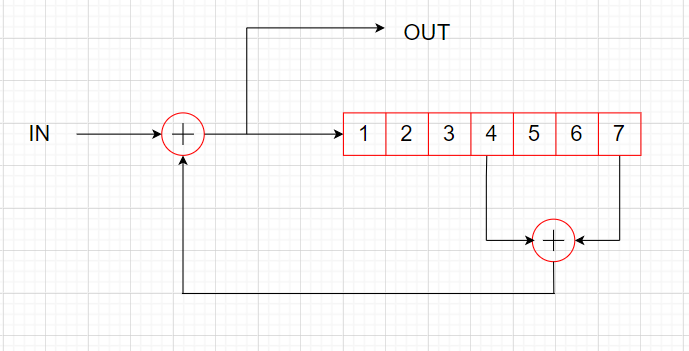
图1 7位乘性加扰器
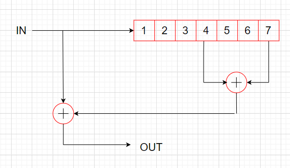
图2 自同步7位乘性解扰器
图1,图2的Verilog RTL 代码如下:
1. 加扰器Verilog 代码:
|
1 2 3 4 5 6 7 8 9 10 11 12 13 14 15 16 17 18 19 20 21 22 23 24 25 26 27 28 29 30 31 32 |
module scrambler ( input clock , // Clock input of the design input rst , // active high, synchronous Reset input input enable , // Active high enable signal input bit_in, // Input data bit. output reg bit_out // Scrambled output bit. ); reg [ 6: 0 ] scb_bit ; always @ ( posedge clock or posedge rst ) if ( rst ) bit_out <= 1'b0; else bit_out <= ( bit_in ^ scb_bit[ 6 ] ^ scb_bit[ 3 ] ); //注意乘性加扰LFSR寄存器不能初始化全1,其它都可以 always @ ( posedge clock or posedge rst ) if ( rst ) begin scb_bit <= 7'b0000000; //Zeroed start. Might be common? //scb_bit <= 7'b1010101; //Striped start. //scb_bit <= 7'b1000101; //Striped start. //scb_bit <= 7'b1111111; //Illegal start. 非法初始化 end else if ( enable == 1'b1 ) begin scb_bit <= { scb_bit[ 5:0 ] , bit_out }; end endmodule |
2. 解扰器Verilog代码:
|
1 2 3 4 5 6 7 8 9 10 11 12 13 14 15 16 17 18 19 20 21 22 23 24 25 26 27 28 29 |
module descrambler ( input clock , // Clock input of the design input rst , // active high, asynchronous Reset input input enable , // Active high enable signal input bit_in, // Input data bit. output reg bit_out // Scrambled output bit. ); reg [ 6: 0 ] scb_bit ; always @ ( posedge clock or posedge rst ) if ( rst ) begin scb_bit <= #1 7'b0000000; end else if ( enable ) begin scb_bit <= { scb_bit[ 5: 0 ], bit_in }; end always @ ( posedge clock or posedge rst ) if ( rst ) bit_out <= 1'b0; else bit_out <= ( bit_in ^ scb_bit[ 6 ] ^ scb_bit[ 3 ] ); endmodule |