
RISC-V CPU中 LOAD, STORE 指令集中对SRAM, 和 GPIO 模块的控制,SRAM ,GPIO 等,都可以看做cpu 的外部存储。在哈佛架构中, 使用数据总线,访存这些外部模块
相关参考文章:
RISC-V 教学教案
GPIO 的地址空间:
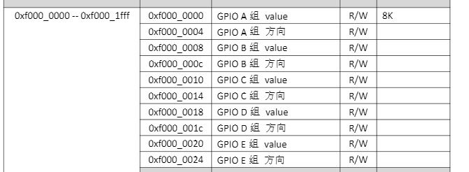
gpio 寄存器地址空间是从0xf000_0000 开始的8k 地址空间。
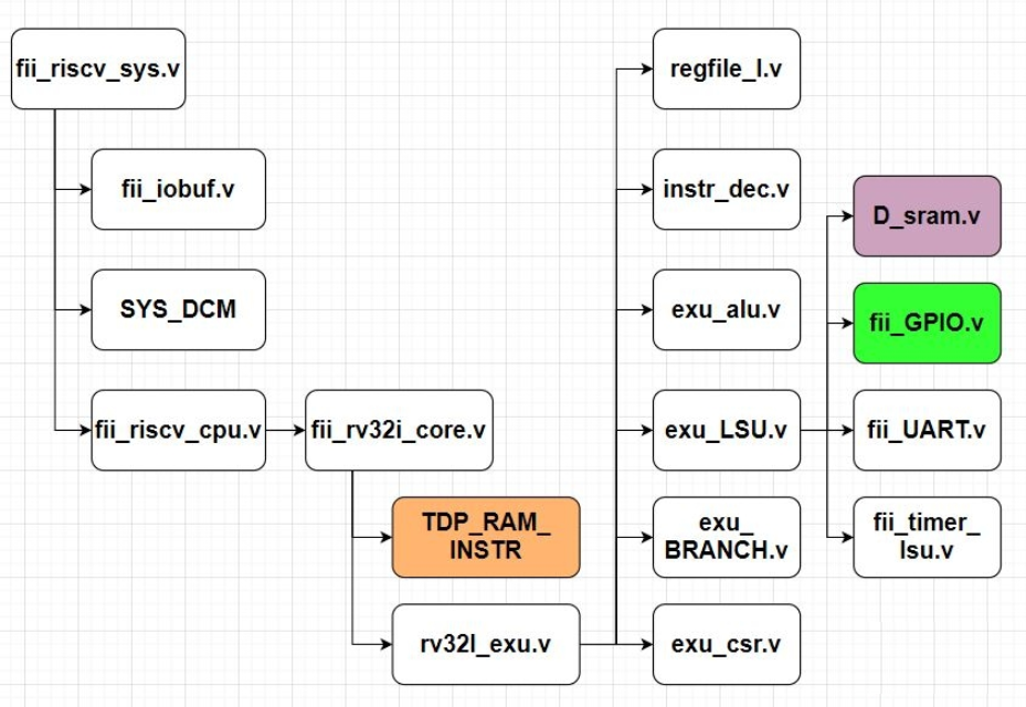
gpio 模块代码:
|
1 2 3 4 5 6 7 8 9 10 11 12 13 14 15 16 17 18 19 20 21 22 23 24 25 26 27 28 29 30 31 32 33 34 35 36 37 38 39 40 41 42 43 44 45 46 47 48 49 50 51 52 53 54 55 56 57 58 59 60 61 62 63 64 65 66 67 68 69 70 71 72 73 74 75 76 77 78 79 80 81 82 83 84 85 86 87 88 89 90 91 92 93 94 95 96 97 98 99 100 101 102 103 104 105 106 107 108 109 110 111 112 113 114 115 116 117 |
module fii_GPIO #( parameter GPIO_DEEP = 8, //memory data width parameter GPIO_W = 32, //memory data width parameter GPIO_MSK_W = 4, //memory data mask width parameter GPIO_ADDR_W = 32 //memory address width ) ( input clk, // 系统时钟 input rst_n, input [ GPIO_W - 1 : 0 ] i_ls_GPIO_din, // cpu 写数据 output [ GPIO_W - 1 : 0 ] o_rb_GPIO_dout, // cpu 读数据 input [ GPIO_ADDR_W - 1 : 0 ] i_addr, // 数据总线地址 input i_cs, // gpio 模块 片选 input i_we, // 写信号 input [ GPIO_MSK_W - 1: 0 ] i_wem, // 写屏蔽信号 // t = 0, output; t = 1, input input [ 31: 0 ] i_GPIO_dina, // gpio 模块a组 cpu写入数据 output [ 31: 0 ] o_GPIO_douta, // gpio 模块a组 cpu读出数据 output [ 31: 0 ] o_GPIO_ta, // gpio 模块a组 方向控制 input [ 31: 0 ] i_GPIO_dinb, // gpio 模块b组 cpu写入数据 output [ 31: 0 ] o_GPIO_doutb, // gpio 模块b组 cpu读出数据 output [ 31: 0 ] o_GPIO_tb, // gpio 模块b组 方向控制 input [ 31: 0 ] i_GPIO_dinc, // gpio 模块c组 cpu写入数据 output [ 31: 0 ] o_GPIO_doutc, // gpio 模块c组 cpu读出数据 output [ 31: 0 ] o_GPIO_tc, // gpio 模块c组 方向控制 input [ 31: 0 ] i_GPIO_dind, // gpio 模块d组 cpu写入数据 output [ 31: 0 ] o_GPIO_doutd, // gpio 模块d组 cpu读出数据 output [ 31: 0 ] o_GPIO_td // gpio 模块d组 方向控制 ); //=============================================================================== reg [ GPIO_W - 1: 0 ] GPIO_r [ 0: GPIO_DEEP - 1 ]; wire [ GPIO_MSK_W - 1: 0 ] wen; wire ren; wire [ 2: 0 ] w_addr = i_addr[ 4: 2 ]; //=============================================================================== assign ren = i_cs & ( ~i_we ); assign wen = ( { GPIO_MSK_W{ i_cs & i_we } } & i_wem ); reg [ GPIO_ADDR_W - 1: 0 ] addr_r = 0; always@( posedge clk ) if ( ren ) addr_r <= i_addr; //=============================================================================== reg [7:0] i = 0; initial begin for ( i = 0; i < GPIO_DEEP; i = i + 1 ) begin:IO_GPIO_INIT GPIO_r[i] <= ~0; end end genvar wi; generate for ( wi = 0; wi < GPIO_MSK_W; wi = wi + 1 ) begin:IO_write always @( posedge clk ) begin if ( wen[ wi ] ) begin GPIO_r[ w_addr ][ 8 * wi + 7: 8 * wi ] <= i_ls_GPIO_din[ 8 * wi + 7: 8 * wi ]; end end end endgenerate //=============================================================================== wire [ GPIO_W - 1: 0 ] dout_pre; wire [ GPIO_W - 1: 0 ] t_pre; wire [ GPIO_W - 1: 0 ] reg_dout; wire [ GPIO_W - 1: 0 ] in_dout[ 0: GPIO_DEEP / 2 - 1 ]; assign in_dout[ 0 ] = i_GPIO_dina; assign in_dout[ 1 ] = i_GPIO_dinb; assign in_dout[ 2 ] = i_GPIO_dinc; assign in_dout[ 3 ] = i_GPIO_dind; //wire [ 31: 0 ] in_dout_tmp = in_dout[ i_addr[ GPIO_DEEP / 2 - 1: 1 ] ]; wire [ 31: 0 ] in_dout_tmp = in_dout[ w_addr[ 2: 1 ]]; //assign t_pre = GPIO_r[ { addr_r[ GPIO_ADDR_W - 1: 1 ], 1'b1 } ]; //assign dout_pre = GPIO_r[ { addr_r[ GPIO_ADDR_W - 1: 1 ], 1'b0 } ]; assign t_pre = GPIO_r[ { w_addr[ 2: 1 ], 1'b1 } ]; assign dout_pre = GPIO_r[ { w_addr[ 2: 1 ], 1'b0 } ]; //=============================================================================== genvar rbi; generate for ( rbi = 0; rbi < GPIO_W; rbi = rbi + 1 ) begin:GPIO_readb // input reg output reg assign o_rb_GPIO_dout[ rbi ] = t_pre[ rbi ] ? in_dout_tmp[ rbi ] : dout_pre[ rbi ]; end endgenerate //=============================================================================== assign o_GPIO_douta = GPIO_r[ 0 ]; assign o_GPIO_ta = GPIO_r[ 1 ]; assign o_GPIO_doutb = GPIO_r[ 2 ]; assign o_GPIO_tb = GPIO_r[ 3 ]; assign o_GPIO_doutc = GPIO_r[ 4 ]; assign o_GPIO_tc = GPIO_r[ 5 ]; assign o_GPIO_doutd = GPIO_r[ 6 ]; assign o_GPIO_td = GPIO_r[ 7 ]; //=============================================================================== endmodule |
端口介绍:
input [ GPIO_W – 1 : 0 ] i_ls_GPIO_din, // cpu 写数据
output [ GPIO_W – 1 : 0 ] o_rb_GPIO_dout, // cpu 读数据
input [ GPIO_ADDR_W – 1 : 0 ] i_addr, // 数据总线地址
input i_cs, // gpio 模块 片选
input i_we, // 写信号
input [ GPIO_MSK_W – 1: 0 ] i_wem, // 写屏蔽信号
input [ 31: 0 ] i_GPIO_dina, // gpio 模块a组 cpu写入数据
output [ 31: 0 ] o_GPIO_douta, // gpio 模块a组 cpu读出数据
output [ 31: 0 ] o_GPIO_ta, // gpio 模块a组 方向控制
input [ 31: 0 ] i_GPIO_dinb, // gpio 模块b组 cpu写入数据
output [ 31: 0 ] o_GPIO_doutb, // gpio 模块b组 cpu读出数据
output [ 31: 0 ] o_GPIO_tb, // gpio 模块b组 方向控制
input [ 31: 0 ] i_GPIO_dinc, // gpio 模块c组 cpu写入数据
output [ 31: 0 ] o_GPIO_doutc, // gpio 模块c组 cpu读出数据
output [ 31: 0 ] o_GPIO_tc, // gpio 模块c组 方向控制
input [ 31: 0 ] i_GPIO_dind, // gpio 模块d组 cpu写入数据
output [ 31: 0 ] o_GPIO_doutd, // gpio 模块d组 cpu读出数据
output [ 31: 0 ] o_GPIO_td // gpio 模块d组 方向控制
定义gpio 寄存器组:
reg [ GPIO_W – 1: 0 ] GPIO_r [ 0: GPIO_DEEP – 1 ];
定义读,写,地址信号:
wire [ GPIO_MSK_W – 1: 0 ] wen;
wire ren;
wire [ 2: 0 ] w_addr = i_addr[ 4: 2 ];
assign ren = i_cs & ( ~i_we );
assign wen = ( { GPIO_MSK_W{ i_cs & i_we } } & i_wem );
gpio 模块寄存器组,写逻辑:
|
1 2 3 4 5 6 7 8 9 10 11 12 13 |
genvar wi; generate for ( wi = 0; wi < GPIO_MSK_W; wi = wi + 1 ) begin:IO_write always @( posedge clk ) begin if ( wen[ wi ] ) begin GPIO_r[ w_addr ][ 8 * wi + 7: 8 * wi ] <= i_ls_GPIO_din[ 8 * wi + 7: 8 * wi ]; end end end endgenerate |
读取gpio组中的方向寄存器, 数据寄存器:
|
1 2 3 4 5 6 7 8 9 10 11 12 13 14 15 |
wire [ GPIO_W - 1: 0 ] dout_pre; wire [ GPIO_W - 1: 0 ] t_pre; wire [ GPIO_W - 1: 0 ] reg_dout; wire [ GPIO_W - 1: 0 ] in_dout[ 0: GPIO_DEEP / 2 - 1 ]; assign in_dout[ 0 ] = i_GPIO_dina; assign in_dout[ 1 ] = i_GPIO_dinb; assign in_dout[ 2 ] = i_GPIO_dinc; assign in_dout[ 3 ] = i_GPIO_dind; wire [ 31: 0 ] in_dout_tmp = in_dout[ w_addr[ 2: 1 ]]; assign <span style="color: #0000ff;">t_pre</span> = GPIO_r[ { w_addr[ 2: 1 ], 1'b1 } ]; // 当前地址选中的GPIO ,A,B,C,D 组中 方向寄存器 assign <span style="color: #0000ff;">dout_pre</span> = GPIO_r[ { w_addr[ 2: 1 ], 1'b0 } ]; // 读取当前地址选中的GPIO ,A,B,C,D 组中gpio 值寄存器 |
cpu 写gpio 寄存器组:
|
1 2 3 4 5 6 7 8 9 10 11 12 13 |
genvar wi; generate for ( wi = 0; wi < GPIO_MSK_W; wi = wi + 1 ) begin:IO_write always @( posedge clk ) begin if ( wen[ wi ] ) begin GPIO_r[ w_addr ][ 8 * wi + 7: 8 * wi ] <= i_ls_GPIO_din[ 8 * wi + 7: 8 * wi ]; end end end endgenerate |
cpu 读取gpio 寄存器组中的内容:
|
1 2 3 4 5 6 7 8 |
genvar rbi; generate for ( rbi = 0; rbi < GPIO_W; rbi = rbi + 1 ) begin:GPIO_readb // input reg output reg assign o_rb_GPIO_dout[ rbi ] = t_pre[ rbi ] ? in_dout_tmp[ rbi ] : dout_pre[ rbi ]; end endgenerate |
当t_pre == 1 时, 读取 input fpga pin 的数值;当t_pre == 0 时, 读取 当前gpio数值寄存器中的值;
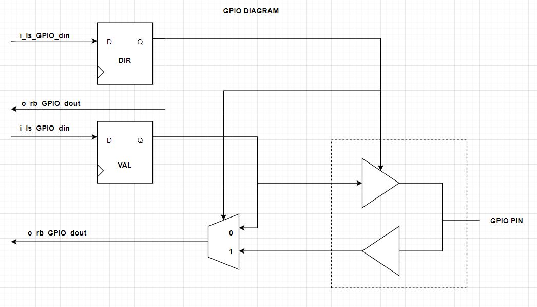
将gpio 寄存器组的相关内容输出到顶层文件的原语中:
assign o_GPIO_douta = GPIO_r[ 0 ];
assign o_GPIO_ta = GPIO_r[ 1 ];
assign o_GPIO_doutb = GPIO_r[ 2 ];
assign o_GPIO_tb = GPIO_r[ 3 ];
assign o_GPIO_doutc = GPIO_r[ 4 ];
assign o_GPIO_tc = GPIO_r[ 5 ];
assign o_GPIO_doutd = GPIO_r[ 6 ];
assign o_GPIO_td = GPIO_r[ 7 ];