
当完成所有uart功能后, 有时,需要将uart模块连接到这个系统中去。 这时,就需要使用寄存器接口来配置uart的不同工作模式。 比如波特率,奇偶校验, 停止位等等信息。这些信息可能在不同的应用场景中动态更改。在这种情况下, 就不能在使用parameter 参数,需要使用模块端口进行动态配置。在cpu设计中,往往使用总线与各个外设进行连接,比如axi 总线,RISCV 的RIB总线,以及自主设计的其他总线等等。不论使用何种总线,在总线中都有data, address,read,write,等信号。本文将已自主设计总线方式,对uart 模块进行设计。
1 系统设计框架
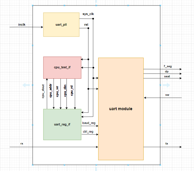
图1
如图1 所示:
1)将PLL 模块从uart module 中移出,放到顶层模块中
2)将parameter更改为模块端口
3)增加uart 寄存器模块,用来连接系统总线和寄存器接口(uart_reg_if.v)
4)增加测试cpu模块,用来验证寄存器相关的读写操作(cpu_test_if.v)

图2
图2中显示各个模块之间详细连接图。
2 uart 模块
uart 模块在之前的文章中都有介绍,在本文中只对接口做了更改。 将parameter 转变为端口输入信号。
3 uart_reg_if 模块
uart_reg_if 模块将接收cpu总线发过来的命令,同时解析cpu命令,确定寄存器地址,读写操作,以及读写的数据。目前在这个模块中设计了2个寄存器,用户可以根据需求,继续增加寄存器。
| 地址 | 寄存器名称 | 注释 |
| 32’he000_0000 | UART_CTRL_REG | uart 模块配置寄存器 |
| 32’he000_0004 | UART_BAUD_REG | uart模块波特率设计寄存器 |
- UART_CTRL_REG
| x | check_sum | x | parity_type | parity | stop_bit |
| bit31-bit5 | bit4 | bit3 | bit2 | bit1 | bit0 |
| no used | 0 => no check sum
1 => enable check sum |
no used | 0 = > even parity
1=> odd parity |
0 => no parity
1 => has parity |
0 => 1 stop bit
1 => 2 stop bit |
- UART_BAUD_REG
| baud tick count | |||||
| bit 31 – 0 | |||||
| default: 625
baud tick count = 72_000_000/baud_rate: for example: 625 = 72_000_000/ 115200 3750 = 72_000_000/ 19200 7500 = 72_000_000/9600 ……. |
uart_reg_if.v 代码:
|
1 2 3 4 5 6 7 8 9 10 11 12 13 14 15 16 17 18 19 20 21 22 23 24 25 26 27 28 29 30 31 32 33 34 35 36 37 38 39 40 41 42 43 44 45 46 47 48 49 50 51 52 53 54 55 56 57 58 59 60 61 62 63 64 65 66 67 68 69 70 71 72 73 74 75 76 77 78 79 80 81 82 83 84 85 86 87 88 89 90 91 92 |
`timescale 1ns / 1ps module uart_reg_if # ( parameter UART_CTRL_REG = 32'he000_0000, parameter UART_BAUD_REG = 32'he000_0004 ) ( input sys_clk, input [31:0] cpu_addr, // cpu address, used for selecting register address input [3:0] cpu_wr, // cpu write, each bit control one byte. for example: cpu_wr = 4'b1100, cpu_din[31:16] will be used to write a register[31:16], cpu_din[15:0] is masked input cpu_rd, // cpu read, cpu_dout is send to cpu input [31:0] cpu_din, // data from cpu output [31:0] cpu_dout, // data will be send to cpu output [31:0] ctrl_reg, // 【0】 : 0 => 1 stop bit ; 1=> 2 stop bit\ 【1】 : 0 => no parity ; 1=> parity\【2】 : 0 => even ; 1=> odd ; output [31:0] baud_reg, // 波特率使能计数器 input rst ); /* ctrl_reg: ================================================================== | check_sum | x | parity type | parity | stop_bit | ================================================================== | bit4 | bit3 | bit 2 | bit 1 | bit0 | ================================================================== baud_reg: ================================================================== | baud tick count | ================================================================== | bit31 - bit0 | ================================================================== | baud tick count = 72_000_000 / baud rate | ================================================================== */ //================================配置uart参数 localparam PARITY = "NONE"; //"ODD"--odd parity, "EVEN"--even parity, others--no parity localparam STOP_BIT = 1; localparam BAUD_RATE = 115200; localparam FREQUENCY = 72_000_000; localparam TX_DIV_COE = FREQUENCY / BAUD_RATE; // write register reg [31:0] baud_reg_r = TX_DIV_COE; always @ (posedge sys_clk or posedge rst) if(rst) baud_reg_r <= TX_DIV_COE; else if(cpu_addr == UART_BAUD_REG) begin if(cpu_wr[0]) baud_reg_r[07:00] <= cpu_din[07:00]; if(cpu_wr[1]) baud_reg_r[15:08] <= cpu_din[15:08]; if(cpu_wr[2]) baud_reg_r[23:16] <= cpu_din[23:16]; if(cpu_wr[3]) baud_reg_r[31:24] <= cpu_din[31:24]; end assign baud_reg = baud_reg_r; reg [31:0] ctrl_reg_r = 0; always @ (posedge sys_clk or posedge rst) if(rst) ctrl_reg_r <= 0; else if(cpu_addr == UART_CTRL_REG) begin if(cpu_wr[0]) ctrl_reg_r[07:00] <= cpu_din[07:00]; if(cpu_wr[1]) ctrl_reg_r[15:08] <= cpu_din[15:08]; if(cpu_wr[2]) ctrl_reg_r[23:16] <= cpu_din[23:16]; if(cpu_wr[3]) ctrl_reg_r[31:24] <= cpu_din[31:24]; end assign ctrl_reg = ctrl_reg_r; // read register reg [31:0] cpu_dout_r = 0; always @ (posedge sys_clk or posedge rst) if(rst) cpu_dout_r <= 0; else if(cpu_rd) begin case(cpu_addr) UART_BAUD_REG: cpu_dout_r <= baud_reg_r; UART_CTRL_REG: cpu_dout_r <= ctrl_reg_r; default: cpu_dout_r <= 0; endcase end assign cpu_dout = cpu_dout_r; endmodule |
端口介绍:
input sys_clk, // 系统时钟
input [31:0] cpu_addr, // cpu 地址总线
input [3:0] cpu_wr, // 4bit cpu 写信号, 适用于32bit 数据总线,每一个bit对应一个数据byte
input cpu_rd, // cpu 读信号
input [31:0] cpu_din, // cpu 写数据到外设
output [31:0] cpu_dout, // cpu 从外设中读取数据
output [31:0] ctrl_reg, // uart 控制寄存器
output [31:0] baud_reg, // 波特率计数器
cpu 写 外设寄存器:
always @ (posedge sys_clk or posedge rst)
if(rst) baud_reg_r <= TX_DIV_COE;
else if(cpu_addr == UART_BAUD_REG)
begin
if(cpu_wr[0]) baud_reg_r[07:00] <= cpu_din[07:00];
if(cpu_wr[1]) baud_reg_r[15:08] <= cpu_din[15:08];
if(cpu_wr[2]) baud_reg_r[23:16] <= cpu_din[23:16];
if(cpu_wr[3]) baud_reg_r[31:24] <= cpu_din[31:24];
end
1)选中寄存器地址,
2)根据不同的写信号 cpu_wr[3:0] ,决定那些数据写入到外设的寄存器中。
cpu 读外设寄存器:
// read register
reg [31:0] cpu_dout_r = 0;
always @ (posedge sys_clk or posedge rst)
if(rst) cpu_dout_r <= 0;
else if(cpu_rd)
begin
case(cpu_addr)
UART_BAUD_REG: cpu_dout_r <= baud_reg_r;
UART_CTRL_REG: cpu_dout_r <= ctrl_reg_r;
default: cpu_dout_r <= 0;
endcase
end
assign cpu_dout = cpu_dout_r;
4 cpu_test_if 模块
模拟cpu 总线,发送地址,读写命令,发送写外设数据,或者读取外设数据。本模块模拟cpu 设置uart_ctrl, uart_baud 寄存器。同时可以读取这2个寄存器。
流程图:
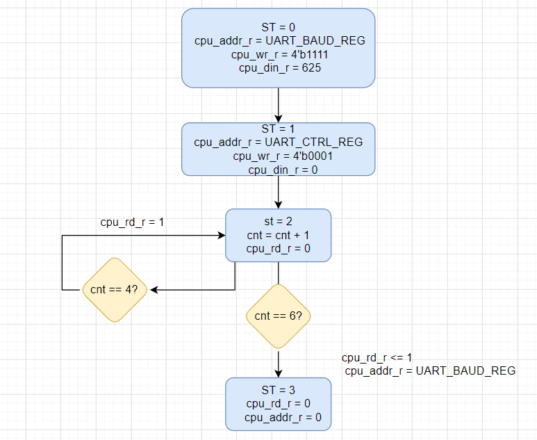
图3
状态机详解:
初始化:rst对模块进行初始化操作
状态0:给出写寄存器地址,写使能,写数据,跳转到状态1
状态1:给出第二个需要写的寄存器地址,写使能,写数据,跳转到状态2
状态2:写使能,写数据清0,开始计数,当计数到4的时候给读使能;计数到6的时候给读使能及读寄存器地址,跳转到状态3
状态3:对各种变量清0,保持状态3
cpu_test_if.v 代码:
|
1 2 3 4 5 6 7 8 9 10 11 12 13 14 15 16 17 18 19 20 21 22 23 24 25 26 27 28 29 30 31 32 33 34 35 36 37 38 39 40 41 42 43 44 45 46 47 48 49 50 51 52 53 54 55 56 57 58 59 60 61 62 63 64 65 66 67 68 69 70 71 72 73 74 75 76 77 78 79 80 81 82 83 84 85 86 87 88 89 90 91 |
`timescale 1ns / 1ps module cpu_test_if # ( parameter UART_CTRL_REG = 32'he000_0000, parameter UART_BAUD_REG = 32'he000_0004 ) ( input sys_clk, output [31:0] cpu_addr, // cpu address, used for selecting register address output [3:0] cpu_wr, // cpu write, each bit control one byte. for example: cpu_wr = 4'b1100, cpu_din[31:16] will be used to write a register[31:16], cpu_din[15:0] is masked output cpu_rd, // cpu read, cpu_dout is send to cpu output [31:0] cpu_din, // data from cpu input [31:0] cpu_dout, // data will be send to cpu input rst ); reg [3:0] cnt; reg [31:0] cpu_addr_r; reg [3:0] cpu_wr_r; reg cpu_rd_r; reg [31:0] cpu_din_r; reg [3:0] wr_st; always@(posedge sys_clk or posedge rst) if(rst) begin cpu_addr_r <= 0; cpu_wr_r <= 0; cpu_din_r <= 0; cnt <= 0; cpu_rd_r <= 0; wr_st <= 0; end else case(wr_st) 0: begin cnt <= 0; cpu_addr_r <= UART_BAUD_REG; cpu_wr_r <= 4'b1111; cpu_din_r <= 625; wr_st <= 1; end 1: begin cpu_addr_r <= UART_CTRL_REG; cpu_wr_r <= 4'b0001; cpu_din_r <= 32'h0000_0000; wr_st <= 2; end 2: begin cpu_rd_r <= 0; cpu_din_r <= 0; cpu_wr_r <= 0; cnt <= cnt + 1; if(cnt == 4) begin cpu_rd_r <= 1; end if(cnt == 6) begin cpu_rd_r <= 1; cpu_addr_r <= UART_BAUD_REG; wr_st <= 3; end end 3: begin wr_st <= 3; cpu_rd_r <= 0; cpu_addr_r <= 0; end default:; endcase assign cpu_addr = cpu_addr_r; assign cpu_wr = cpu_wr_r; assign cpu_rd = cpu_rd_r; assign cpu_din = cpu_din_r; endmodule |
5 仿真及下载调试
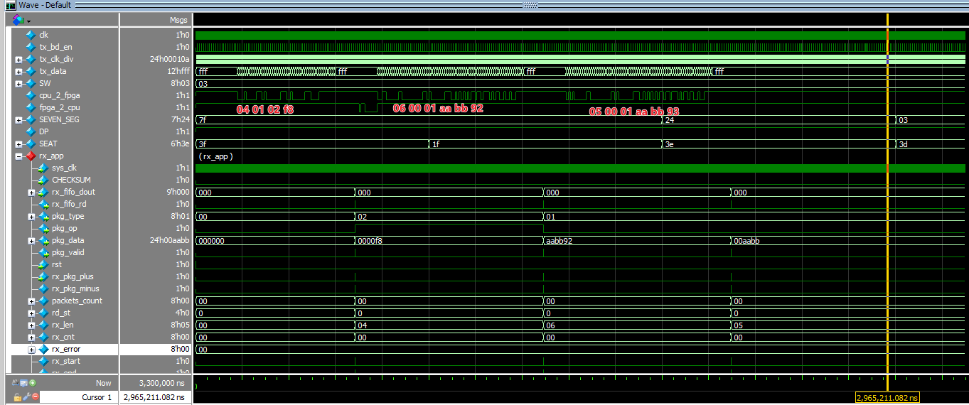
图4
测试波形,模拟cpu端发送, 波特率115200, 8bit, no parity, 1 stop bit。 test1: 04 01 02 f8(截断测试) test2: 06 00 01 aa bb 92 test3: 05 00 01 aa bb 93 (截断测试)
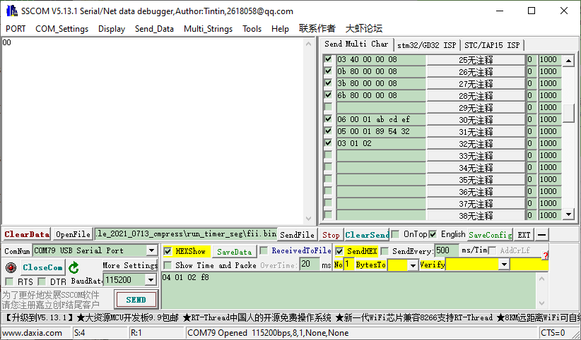
图5
下板测试 04 01 02 f8 (截断测试) 整个数据包完整,读取波段开关只需要3 个字节。 即: 03 01 02 即可。 使用4 个字节,FPGA 可以截断有效字节。
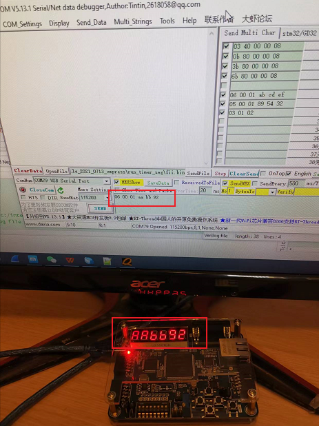
图6
测试06 00 01 aa bb 92 ,完整数据包, 在pra006 上显示正确。
quartus 工程代码:
[content_control]
uart_fifo_checksum_cputest.zip
[/content_control]