
在讲解清楚了通信分层的概念和PCS子层编码后,由于发送端的PCS子层采用8b/10b编码,因此接收端的对应层也要采用相同的解码方式。通信工程的各个分层如图1所示。
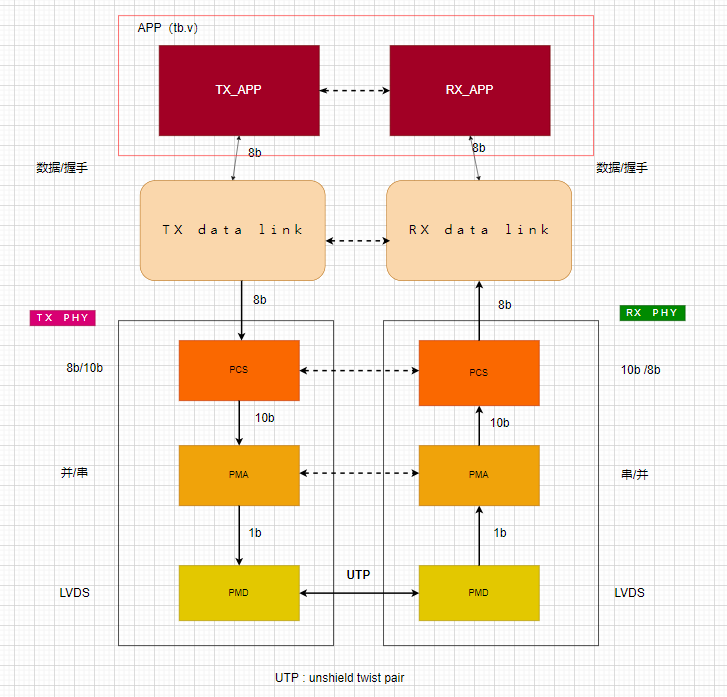
图1 高速通信分层的概念
本节内容除了添加了PCS子层外,还将整个工程接收部分的代码做了较大修改,使得工程中的层次更加分明,但要注意各个层之间的握手。各层的代码如下:
1. 接收端PMD层
这段代码和以前的代码一样,只是文件名做了修改,体现了该代码所在的层次。本层的任务是完成LVDS到单端信号的变换,并将接收 bit流通过本地时钟过采样,进行相位自适应调整,同步到本地时钟域。
|
1 2 3 4 5 6 7 8 9 10 11 12 13 14 15 16 17 18 19 20 21 22 23 24 25 26 27 28 29 30 31 32 33 34 35 36 37 38 39 40 41 42 43 44 45 46 47 48 49 50 51 52 53 54 55 56 57 58 59 60 61 62 63 64 65 66 67 68 69 70 71 72 73 74 75 76 77 |
module recv_bit_pmd ( input rst, input clk_400M , //400Hz input rx, output reg rx_bit, output reg rx_bit_rdy, output reg rx_r, //r---register output reg rx_rr, //rr--- rx_r registerd output reg rx_dg //dg----double (dual) edge, 上升沿或下降沿 ); ////=========rx_xx[0]^rx_xx[1]==1,dual edge wire rx_out; reg rx_rrr; reg [ 1: 0 ] sample_count = 0; always@( posedge clk_400M or posedge rst ) if ( rst ) begin rx_r <= 0; rx_rr <= 0; rx_rrr <= 0; rx_dg <= 0; end else begin rx_r <= rx_out; rx_rr <= rx_r; rx_rrr <= rx_rr; rx_dg <= rx_r ^ rx_rr; //dual edge end always@( posedge clk_400M or posedge rst ) if ( rst ) begin rx_bit_rdy <= 0; rx_bit <= 0; sample_count <= 0; end else begin rx_bit_rdy <= 0; if ( sample_count == 2 ) //0, 1 ,2 ,3 ,0,1,2,3.。。。 begin rx_bit <= rx_rrr; // rx_bit_rdy <= 1'b1; end if ( rx_dg ) // 2 3 0 0 begin sample_count <= 0; end else begin sample_count <= sample_count + 1'b1; end end IO_RX IO_RX_inst ( .rx_in ( rx ), .rx_out ( rx_out ) ); endmodule |
2. 接收端PMA层代码
本层代码由于采用了8b/10b编码的方式,按照约定,发送端的PCS子层封装数据包时采用K28.5作为帧start,K28.1作为帧end (stop)。由于8b/10b的优良特性,K28.5和K28.1是8b/10b中的逗号,在编码码字中含有连续的5个0或5个1, 而且码字在整个串行流是惟一的。因此可以直接捕获K28.5和K28.1的10-bit数据代替Preamble + SFD作为同步字使用。其它的如寄存器移位,异步时钟的转换等,见上几个章节的介绍。最终输出3个信号rx_data_100Mr, rx_data_rdy_100Mr, rx_data_vld_pma用于与上层的握手。见仿真波形图2,3 ,4。
|
1 2 3 4 5 6 7 8 9 10 11 12 13 14 15 16 17 18 19 20 21 22 23 24 25 26 27 28 29 30 31 32 33 34 35 36 37 38 39 40 41 42 43 44 45 46 47 48 49 50 51 52 53 54 55 56 57 58 59 60 61 62 63 64 65 66 67 68 69 70 71 72 73 74 75 76 77 78 79 80 81 82 83 84 85 86 87 88 89 90 91 92 93 94 95 96 97 98 99 100 101 102 103 104 105 106 107 108 109 110 111 112 113 114 115 116 117 118 119 120 121 122 123 124 125 126 127 128 129 130 131 132 133 134 135 136 137 138 139 140 141 142 143 144 145 146 147 148 149 150 151 152 153 154 155 156 157 158 159 160 161 162 163 164 165 166 167 168 169 170 171 172 173 174 175 176 177 178 179 |
module recv_data_pma #( parameter SYNC_START1 = 10'b0011111010, //K28.5 with dipin=0; parameter SYNC_START2 = 10'b1100000101, //K28.5 with dispin=1 parameter SYNC_END1 = 10'b0011111001, //K28.1 with dipin=0; parameter SYNC_END2 = 10'b1100000110 //K28.1 with dispin=1 ) ( input rst, input clk_100M , input clk_400M , input rx, output reg[ 9: 0 ] rx_data_100Mr, output reg rx_data_rdy_100Mr, output reg rx_data_vld_pma ); wire rx_bit; wire rx_bit_rdy; reg [ 3: 0 ] bit_count; reg [ 9: 0 ] bit_sft; reg fr_sync1; reg fr_sync; reg fr_end; reg[ 9: 0 ] rx_data; reg rx_data_rdy; always@( posedge clk_400M or posedge rst ) if ( rst ) begin rx_data <= 0; rx_data_rdy <= 0; bit_count <= 0; bit_sft <= 0; fr_sync1 <= 0; fr_sync <= 0; fr_end <= 0; end else begin if ( rx_bit_rdy ) bit_sft <= { bit_sft[ 8: 0 ], rx_bit }; if ( fr_end ) fr_sync1 <= 1'b0; else if ( ( bit_sft == SYNC_START1 ) || ( bit_sft == SYNC_START2 ) ) fr_sync1 <= 1'b1; if ( fr_end ) fr_sync <= 1'b0; else if ( fr_sync1 & rx_bit_rdy ) fr_sync <= 1'b1; if ( fr_end ) bit_count <= 0; else if ( fr_sync ) begin if ( rx_bit_rdy ) begin if ( bit_count == 9 ) bit_count <= 0; else bit_count <= bit_count + 1; end end rx_data_rdy <= 0; if ( bit_count == 9 ) begin rx_data <= bit_sft; rx_data_rdy <= 1'b1; end fr_end <= 1'b0; if ( ( bit_sft == SYNC_END1 ) || ( bit_sft == SYNC_END2 ) ) fr_end <= 1'b1; end reg rx_data_rdy_r; reg [ 5: 0 ] count_400M; reg rx_data_rdy_x; reg nrx_data_rdy_x; reg rx_data_rdy_xrg; always@( posedge clk_400M or posedge rst ) if ( rst ) begin count_400M <= 0; rx_data_rdy_r <= 0; end else begin if ( rx_data_rdy ) rx_data_rdy_r <= 1'b1; else if ( count_400M == 19 ) rx_data_rdy_r <= 1'b0; if ( count_400M == 19 ) count_400M <= 0; else if ( rx_data_rdy_r ) count_400M <= count_400M + 1; end always@( posedge clk_100M or posedge rst ) if ( rst ) begin rx_data_rdy_x <= 1'b0; nrx_data_rdy_x <= 1'b1; rx_data_rdy_xrg <= 1'b0; rx_data_100Mr <= 0; rx_data_rdy_100Mr <= 1'b0; end else begin rx_data_rdy_x <= rx_data_rdy_r; nrx_data_rdy_x <= !rx_data_rdy_x; rx_data_rdy_xrg <= nrx_data_rdy_x & rx_data_rdy_x; rx_data_rdy_100Mr <= 1'b0; if ( rx_data_rdy_xrg ) begin rx_data_100Mr <= rx_data; rx_data_rdy_100Mr <= 1'b1; end end reg rx_data_vld_x; always@( posedge clk_100M or posedge rst ) if ( rst ) begin rx_data_vld_pma <= 0; end else begin rx_data_vld_x <= fr_sync; rx_data_vld_pma <= rx_data_vld_x; end recv_bit_pmd recv_bit_pmd_inst ( .rst ( rst ), .clk_400M ( clk_400M ), .rx ( rx ), .rx_bit ( rx_bit ), .rx_bit_rdy ( rx_bit_rdy ) ); endmodule |
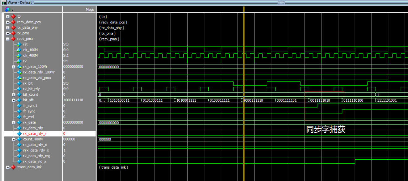
图2 PMA层同步字(K28.5)捕获
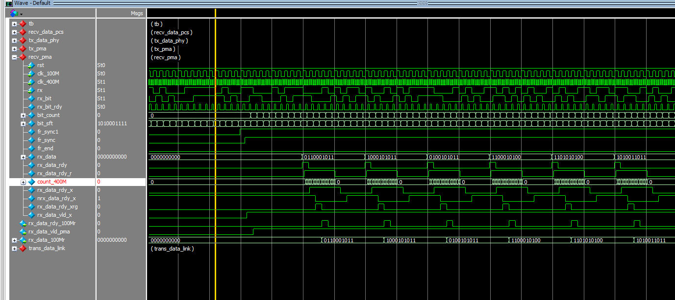
图3 PMA层的时钟域转换及握手信号
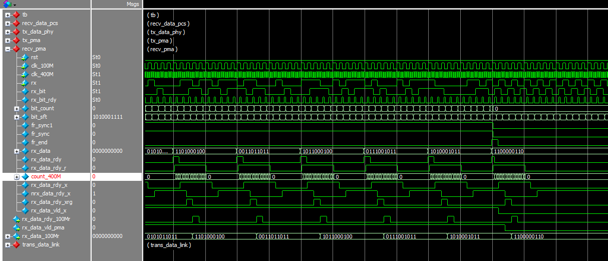
图4 PMA层的时钟域转换及握手信号
3. 接收端PCS代码
|
1 2 3 4 5 6 7 8 9 10 11 12 13 14 15 16 17 18 19 20 21 22 23 24 25 26 27 28 29 30 31 32 33 34 35 36 37 38 39 40 41 42 43 44 45 46 47 48 49 50 51 52 53 54 55 56 57 58 59 60 61 62 63 64 65 66 67 68 69 70 71 72 73 74 75 76 77 78 79 80 81 82 83 84 85 86 87 88 89 90 91 92 93 94 95 96 97 98 99 100 101 102 103 104 105 106 107 108 109 110 111 112 113 114 115 116 117 118 119 120 121 122 123 124 125 126 127 128 129 130 131 132 133 134 135 136 137 138 |
module recv_data_pcs #( parameter SYNC_START1 = 10'b0011111010, //K28.5 with dipin=0; parameter SYNC_START2 = 10'b1100000101, //K28.5 with dispin=1 parameter SYNC_END1 = 10'b0011111001, //K28.1 with dipin=0; parameter SYNC_END2 = 10'b1100000110 //K28.1 with dispin=1 ) ( input rst, input clk_100M , input clk_400M , input rx, output reg pcs_ko, output reg[ 7: 0 ] pcs_rx_data, output reg pcs_rx_data_rdy, output reg pcs_rx_data_vld ); wire code_err; wire disp_err; wire [ 7: 0 ] dataout; wire dispout; wire ko; wire rx_data_rdy_100M; wire rx_data_vld_pma; wire [ 9: 0 ] rx_data_100M; reg dispin; reg [ 9: 0 ] rx_data_100M_r; always@( posedge clk_100M or posedge rst ) if ( rst ) begin pcs_rx_data_vld <= 0; end else pcs_rx_data_vld <= rx_data_vld_pma; reg [ 1: 0 ] pcs_rx_st; always@( posedge clk_100M or posedge rst ) if ( rst ) begin rx_data_100M_r <= 0; dispin <= 0; pcs_ko <= 0; pcs_rx_data <= 0; pcs_rx_data_rdy <= 0; pcs_rx_st <= 0; end else case ( pcs_rx_st ) 0: begin //rx_data_100M_r<=0; //dispin <=0; pcs_ko <= 0; pcs_rx_data <= 0; pcs_rx_data <= 0; pcs_rx_data_rdy <= 0; if ( rx_data_vld_pma ) pcs_rx_st <= 1; end 1: begin pcs_rx_data_rdy <= 0; if ( rx_data_rdy_100M ) begin rx_data_100M_r <= rx_data_100M; pcs_rx_st <= 2; end else if ( !rx_data_vld_pma ) pcs_rx_st <= 0; end 2: begin pcs_ko <= ko; pcs_rx_data <= dataout; dispin <= dispout; pcs_rx_data_rdy <= 1'b1; if ( !rx_data_vld_pma ) pcs_rx_st <= 0; else pcs_rx_st <= 1; end default: pcs_rx_st = 0; endcase decode_10b8b decode_10b8b_inst ( .datain ( rx_data_100M_r ), .dispin ( dispin ), .ko ( ko ), .dataout ( dataout ), .dispout ( dispout ), .code_err ( code_err ), .disp_err ( disp_err ) ) ; recv_data_pma #( .SYNC_START1 ( SYNC_START1 ), //K28.5 with dipin=0; .SYNC_START2 ( SYNC_START2 ), //K28.5 with dispin=1 .SYNC_END1 ( SYNC_END1 ), //K28.5 with dipin=0; .SYNC_END2 ( SYNC_END2 ) //K28.5 with dispin=1 ) recv_data_pma_inst ( .rst ( rst ), .clk_100M ( clk_100M ), .clk_400M ( clk_400M ), .rx ( rx ), .rx_data_100Mr ( rx_data_100M ), .rx_data_rdy_100Mr ( rx_data_rdy_100M ), .rx_data_vld_pma ( rx_data_vld_pma ) ); endmodule |
接收端的数据链路层没有添加 Preamble + SFD 以及FCS, 因此数据链路层的数据和PCS的代码一致,后续课程中会添加相关的应用,进而逐步完善通信工程。握手及10b/8b的转换见图5,6,7。
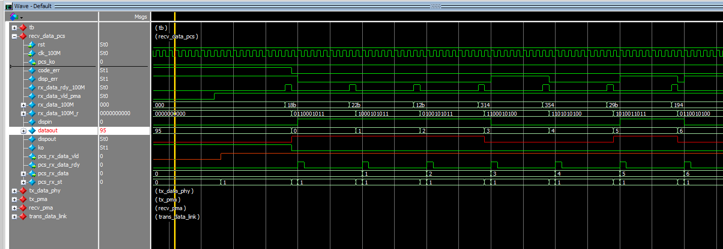
图5 PCS层的时钟域转换及握手信号
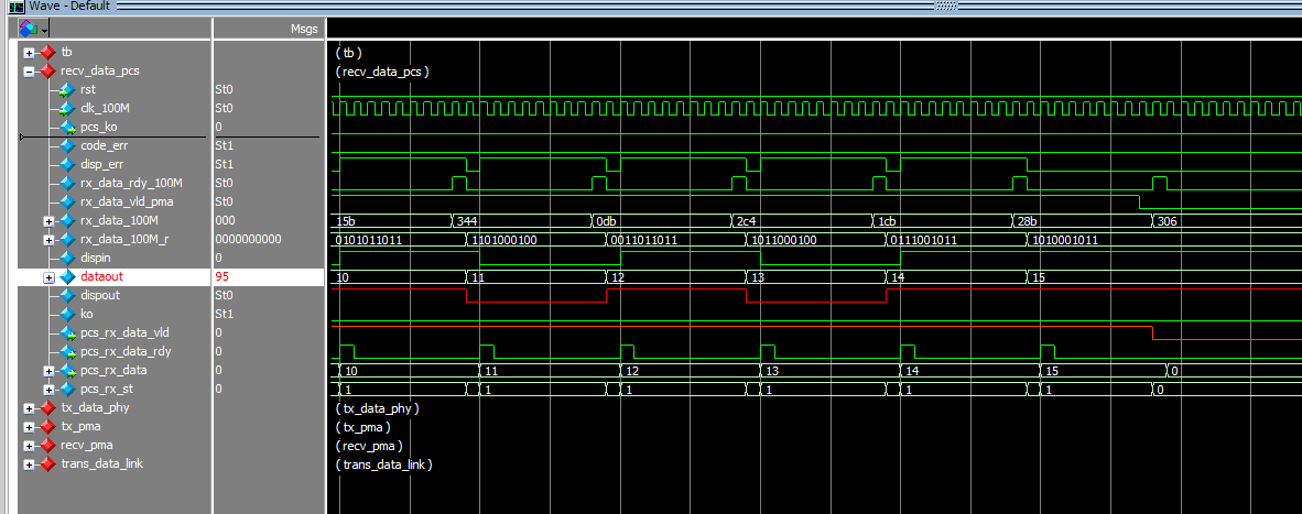
图6 PCS层的时钟域转换及握手信号
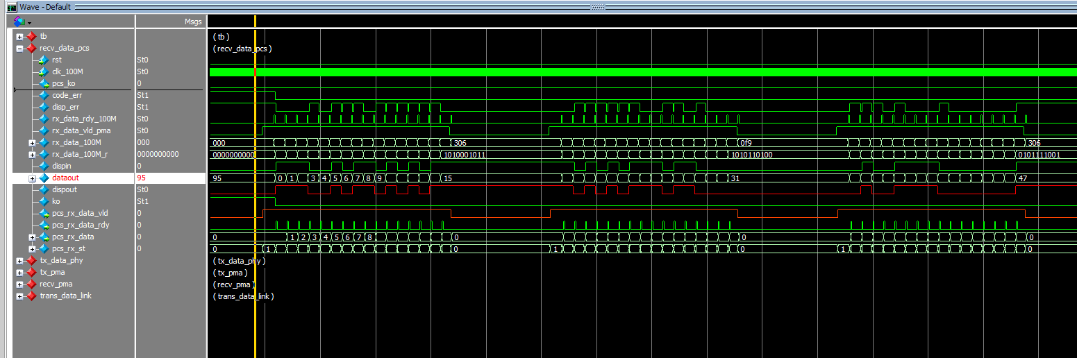
图7 PCS层的时钟域转换及握手信号
由于文章中无法详细展示代码设计及仿真中的细节,如果想了解细节请参照对应视频。
工程代码(quartus 20.1):
[content_control]
[/content_control]