
在之前的几节内容中我们研究了通信分层的概念和分层实现的优点,其中在物理层中有一个非常重要的子层PCS(Physical Coding Sublayer)。该层主要有两个功能:
(1)通过编码实现改善信道的质量,如改善直流平衡,提供足够多的时钟信息等;
(2)提供物理层通信控制功能,实现高层协议无法完成的或不需要高层参与完成的功能。如物理层的自动协商,实现物理层差异时的自动适配,如速率适配,线序调换等功能。
本节内容以8b/10b编码编码框架实现PCS子层,工程代码也做了较大修改充分体现了高速通信中分层的概念。高速通信收发层次如图1所示。
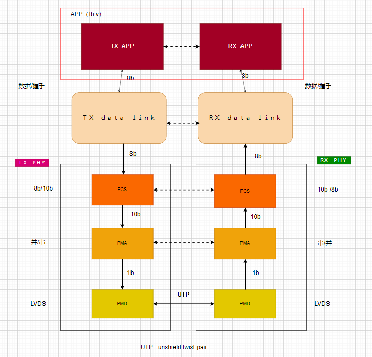
图1
由于整个工程的代码层次比较多,本节内容着重以发送端的代码介绍为主,接收端的代码安排在下节内容实现。在本节内容除了PCS子层代码外,其它内容及实现方法已经介绍,但为了通信工程的层次更加清晰,各层代码也做了较大修改,同时应注重研究在同步时钟域下各层握手的实现方法。
tx握手信号如图2所示。

图2-1 tx握手信号

图2-2 tx握手信号
1. 应用层(tb_8b10b.v)
该层在本阶段作为通信部分研究的最高层,其它的通信协议会在后续的章节中作为扩展部分介绍。
|
1 2 3 4 5 6 7 8 9 10 11 12 13 14 15 16 17 18 19 20 21 22 23 24 25 26 27 28 29 30 31 32 33 34 35 36 37 38 39 40 41 42 43 44 45 46 47 48 49 50 51 52 53 54 55 56 57 58 59 60 61 62 63 64 65 66 67 68 69 70 71 72 73 74 75 76 77 78 79 80 81 82 83 84 85 86 87 88 89 90 91 92 93 94 95 96 97 98 99 100 101 102 103 104 105 106 107 108 109 110 111 112 113 114 115 116 117 118 119 120 121 122 123 124 125 126 127 128 129 130 131 132 133 134 135 136 137 138 139 140 141 142 143 144 145 146 147 148 149 150 151 152 |
`timescale 1 ns / 1 ps module tb_8b10b ( ); parameter LEN = 16; parameter PERIOD = 20 ; //周期20 parameter IDLE = 10'b1010_1010_10; reg inclk ; // 模拟板级提供的输入时钟 initial begin inclk = 1'b0; #( PERIOD / 2 ); forever #( PERIOD / 2 ) inclk = ~inclk; end reg pll_rst; //实体模块PLL的rst信号 wire tx_rx; // 收发在testbench的回环信号 wire clk_100M; wire pll_locked; //实体PLL锁定信号 wire rst = !pll_locked; //Testbench内生成复位信号 reg [ 7: 0 ] tx_data; //待发送数据 wire rx_data_vld; wire rx_data_rdy; wire ko; wire [ 7: 0 ] rx_data; wire tx_rdy; reg tx_vld; reg tx_en; wire tx_vld_ack; reg [ 7: 0 ] frame_len; reg [ 2: 0 ] tx_st; initial begin pll_rst = 1'b1; #50 pll_rst = 1'b0; end always@( posedge clk_100M or posedge rst ) if ( rst ) begin tx_vld <= 1'b0; tx_en <= 1'b0; frame_len <= 0; tx_data <= 0; tx_st <= 0; end else begin case ( tx_st ) 0: begin tx_vld <= 1'b0; tx_en <= 1'b0; tx_data <= 0; frame_len <= 0; tx_st <= 1; end 1: begin tx_en <= 1'b0; tx_vld <= 1'b1; if ( frame_len == LEN ) begin tx_vld <= 1'b0; tx_st <= 3; end else if ( tx_rdy ) begin tx_en <= 1'b1; tx_st <= 2; end end 2: begin tx_en <= 1'b0; frame_len <= frame_len + 1; tx_data <= tx_data + 1; tx_st <= 1; end 3: begin frame_len <= 0; tx_vld <= 1'b0; tx_en <= 1'b0; if ( tx_vld_ack ) tx_st <= 1; end default: tx_st <= 0; endcase end hs_txrx #( .IDLE( IDLE ) ) hs_txrx_inst ( .inclk ( inclk ), .pll_rst ( pll_rst ), .tx_rdy ( tx_rdy ), .tx_vld ( tx_vld ), .tx_data ( tx_data ), .tx_en ( tx_en ), .tx_vld_ack ( tx_vld_ack ), .tx ( tx_rx ), .rx ( tx_rx ), .rx_data_vld( rx_data_vld ), .rx_data_rdy( rx_data_rdy ), .ko ( ko ), .rx_data ( rx_data ), .clk_100M ( clk_100M ), .pll_locked ( pll_locked ) ); endmodule |
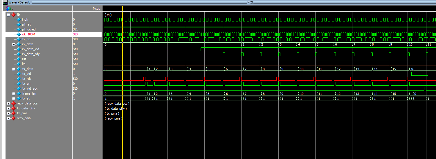
图3 tb_8b10b.v 仿真波形1
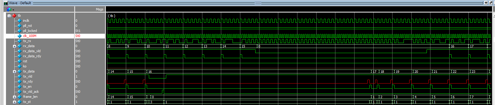
图4 tb_8b10b.v 仿真波形2
2. 高速通信的顶层文件
|
1 2 3 4 5 6 7 8 9 10 11 12 13 14 15 16 17 18 19 20 21 22 23 24 25 26 27 28 29 30 31 32 33 34 35 36 37 38 39 40 41 42 43 44 45 46 47 48 49 50 51 52 53 54 55 56 57 58 59 60 61 62 63 64 65 66 67 68 69 70 71 72 73 74 75 76 77 78 79 80 |
module hs_txrx #( parameter IDLE = 10'b1010_1010_10 ) ( input inclk, input pll_rst, output tx_rdy, input tx_vld, input [ 7: 0 ] tx_data, input tx_en, output tx_vld_ack, output tx, input rx, output rx_data_vld, output rx_data_rdy, output ko, output [ 7: 0 ] rx_data, output clk_100M, output pll_locked ); wire clk_400M; wire rst = !pll_locked; trans_data_link #( .IDLE ( IDLE ) ) trans_data_link_inst ( .rst ( rst ), .clk_100M ( clk_100M ), .tx_rdy ( tx_rdy ), .tx_vld ( tx_vld ), .tx_data ( tx_data ), .tx_en ( tx_en ), .tx_vld_ack ( tx_vld_ack ), .tx_out ( tx ) ); recv_data_pcs # ( .SYNC_START1 ( 10'b0011111010 ), //K28.5 with dipin=0; .SYNC_START2 ( 10'b1100000101 ), //K28.5 with dispin=1 .SYNC_END1 ( 10'b0011111001 ), //K28.5 with dipin=0; .SYNC_END2 ( 10'b1100000110 ) //K28.5 with dispin=1 ) recv_data_pcs_inst ( .rst ( rst ), .clk_100M ( clk_100M ), .clk_400M ( clk_400M ), .rx ( rx ), .pcs_rx_data_rdy ( rx_data_rdy ), .pcs_ko ( ko ), .pcs_rx_data ( rx_data ), .pcs_rx_data_vld ( rx_data_vld ) ); pll1 pll1_inst ( .areset ( pll_rst ), //1'b0; .inclk0 ( inclk ), .c0 ( clk_100M ), .c1 ( clk_400M ), .locked ( pll_locked ) ); endmodule |
3.发送端数据链路层代码
数据链路层(data-link)的上层是应用层,下层为物理层,直接对接的是物理层的PCS子层。注意上下层之间的握手。同时该层包间隔的设定,为了简化设计,Peamble+SFD部分没有插入,感兴趣的读者可以自己尝试。
|
1 2 3 4 5 6 7 8 9 10 11 12 13 14 15 16 17 18 19 20 21 22 23 24 25 26 27 28 29 30 31 32 33 34 35 36 37 38 39 40 41 42 43 44 45 46 47 48 49 50 51 52 53 54 55 56 57 58 59 60 61 62 63 64 65 66 67 68 69 70 71 72 73 74 75 76 77 78 79 80 81 82 83 84 85 86 87 88 89 90 91 92 93 94 95 96 97 98 99 100 101 102 103 104 105 106 107 108 109 110 111 112 113 114 115 116 117 118 119 120 121 122 123 124 125 126 127 128 129 130 131 132 133 134 135 136 137 138 139 140 141 142 143 144 145 146 147 148 149 150 151 152 153 154 155 156 157 |
module trans_data_link #( parameter IDLE = 10'b1010_1010_10 ) ( input rst, input clk_100M, output reg tx_rdy, input tx_vld, input [ 7: 0 ] tx_data, input tx_en, output reg tx_vld_ack, output tx_out ); localparam INTER_PAC_INTERVAL= 96; //packect interval wire tx_phy_rdy; reg tx_phy_rdy_r; reg tx_phy_rdy_ack; always@( posedge clk_100M or posedge rst ) if ( rst ) begin tx_phy_rdy_r <= 0; end else begin if ( tx_phy_rdy ) tx_phy_rdy_r <= 1'b1; else if ( tx_phy_rdy_ack ) tx_phy_rdy_r <= 1'b0; end reg [ 7: 0 ] tx_phy_data; reg tx_phy_en; reg tx_phy_vld; reg [ 7: 0 ] pac_interval; reg [ 2: 0 ] link_st; always@( posedge clk_100M or posedge rst ) if ( rst ) begin pac_interval <= 0; tx_rdy <= 0; tx_phy_data <= 0; tx_phy_vld <= 0; tx_phy_en <= 0; tx_phy_rdy_ack <= 0; tx_vld_ack <= 0; link_st <= 0; end else case ( link_st ) 0: begin tx_phy_data <= 0; tx_phy_vld <= 0; tx_phy_en <= 0; tx_vld_ack <= 0; if ( pac_interval == INTER_PAC_INTERVAL) link_st <= 1; else pac_interval <= pac_interval + 1; end 1: begin pac_interval <= 0; if ( tx_vld ) begin tx_phy_vld <= 1'b1; end if ( tx_phy_rdy ) begin tx_rdy <= 1'b1; link_st <= 2; end end 2: begin tx_rdy <= 1'b0; if ( tx_en ) begin tx_phy_data <= tx_data; link_st <= 3; end end 3: begin if ( tx_phy_rdy_r ) begin tx_phy_en <= 1'b1; tx_phy_rdy_ack <= 1'b1; link_st <= 4; end end 4: begin tx_phy_en <= 1'b0; tx_phy_rdy_ack <= 1'b0; if ( tx_vld ) begin tx_rdy <= 1'b1; link_st <= 2; end else begin tx_vld_ack <= 1'b1; link_st <= 0; end end default: link_st <= 0; endcase tx_data_phy #( .IDLE( IDLE ) ) tx_data_phy_inst ( .rst ( rst ), .clk_100M ( clk_100M ), .tx_phy_rdy ( tx_phy_rdy ), .tx_phy_vld ( tx_phy_vld ), .tx_phy_en ( tx_phy_en ), .tx_phy_data ( tx_phy_data ), .tx_out ( tx_out ) ); endmodule |
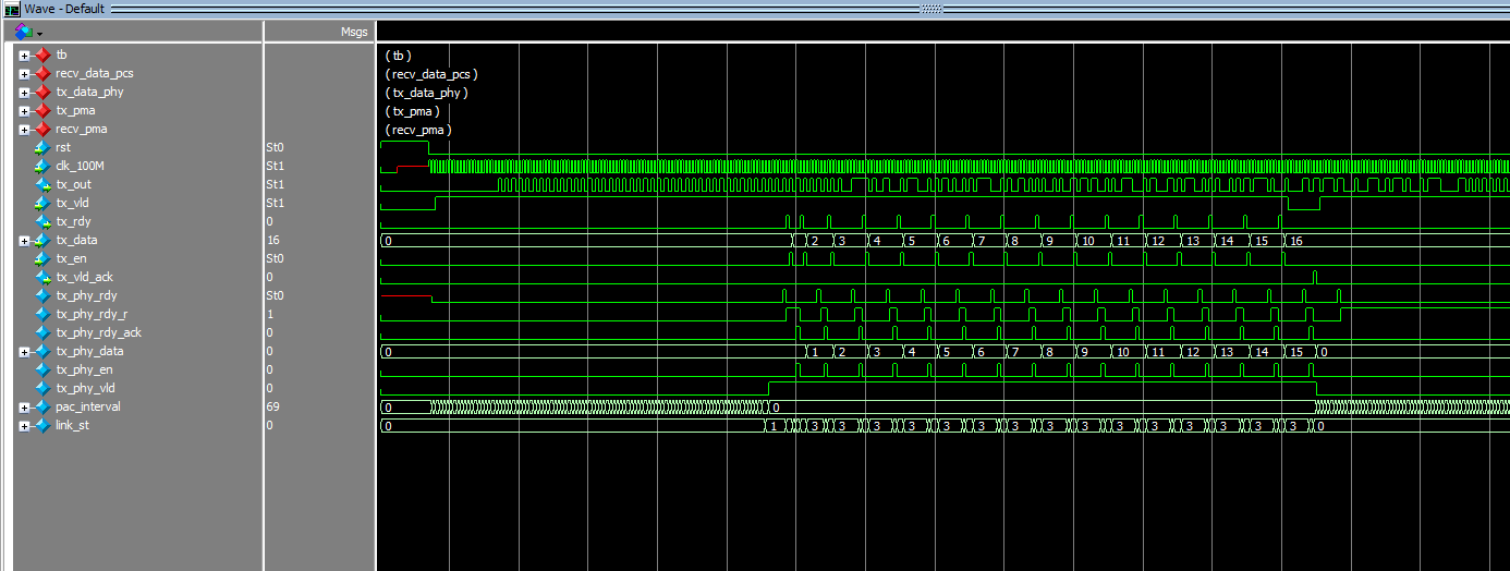
图5 trans_data_link.v 握手信号波形
图5中,应注重观察 data-link 层与应用层及PCS的握手,同时分析包间隔(frame interval)的插入。
4.发送端PCS子层代码
本层的上层是数据链路层,下层为PMA子层,应注意上下层之间的握手。PCS子层采用8b/10b编码实现。其中采用k28.5作为帧起始,K28.1作为帧结束。8b/10b编码部分见 文章 Verilog 8b/10b encoder.
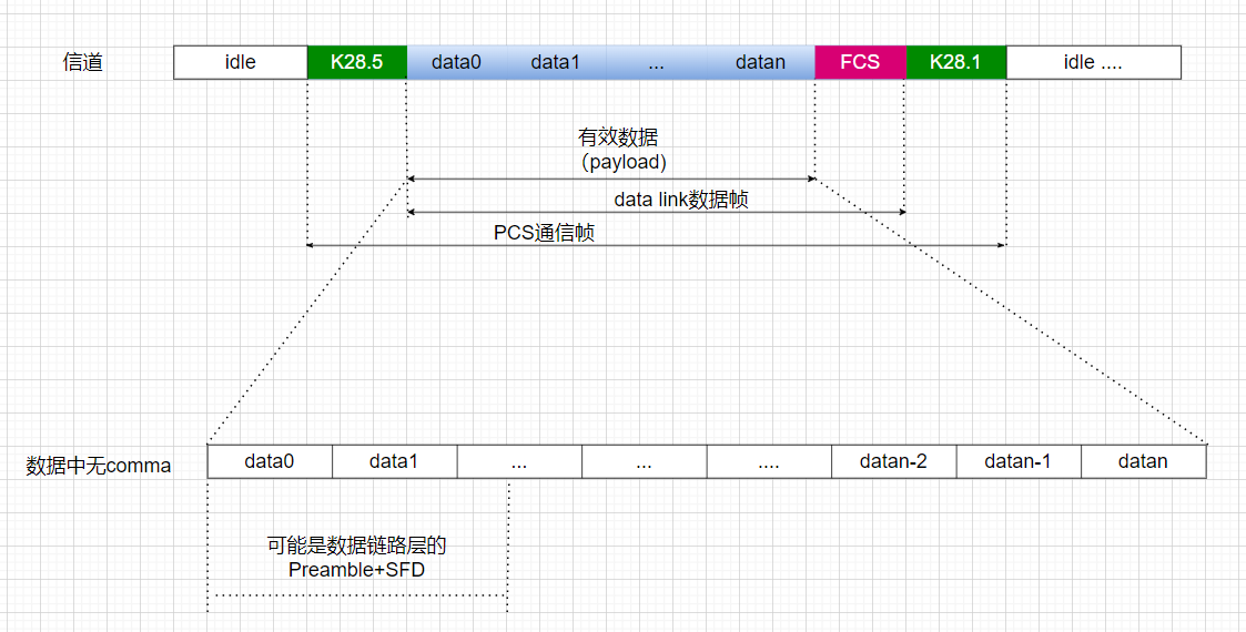
图6
|
1 2 3 4 5 6 7 8 9 10 11 12 13 14 15 16 17 18 19 20 21 22 23 24 25 26 27 28 29 30 31 32 33 34 35 36 37 38 39 40 41 42 43 44 45 46 47 48 49 50 51 52 53 54 55 56 57 58 59 60 61 62 63 64 65 66 67 68 69 70 71 72 73 74 75 76 77 78 79 80 81 82 83 84 85 86 87 88 89 90 91 92 93 94 95 96 97 98 99 100 101 102 103 104 105 106 107 108 109 110 111 112 113 114 115 116 117 118 119 120 121 122 123 124 125 126 127 128 129 130 131 132 133 134 135 136 137 138 139 140 141 142 143 144 145 146 147 148 149 150 151 152 153 154 155 156 157 158 159 160 161 162 163 164 165 166 167 168 169 170 171 172 173 174 175 176 177 178 179 180 181 182 183 184 185 186 187 188 189 190 191 192 193 194 195 196 197 |
/* physcal layer : (1) first layer of physical, PCS sublayer (2) PCS controled through 8b/10b encode (3) engineer: Tim zhuang company : Fraser innovation Inc. */ module tx_data_phy #( parameter IDLE = 10'b10_1010_1010 ) ( input rst, input clk_100M, input tx_phy_vld, output reg tx_phy_rdy, input tx_phy_en, input [ 7: 0 ] tx_phy_data, output tx_out ); reg ki = 0; reg [ 7: 0 ] datain; reg dispin; wire [ 9: 0 ] dataout; wire dispout; reg tx_pcs_en; reg [ 9: 0 ] tx_pcs_data; reg tx_pcs_rdy; reg [ 2: 0 ] pcs_st; always@( posedge clk_100M or posedge rst ) if ( rst ) begin ki <= 0; datain <= 0; dispin <= 0; tx_pcs_en <= 0; tx_pcs_data <= 0; pcs_st <= 0; end else case ( pcs_st ) 0: begin ki <= 0; datain <= 0; dispin <= 0; tx_pcs_en <= 0; tx_pcs_data <= 0; tx_phy_rdy <= 1'b0; if ( tx_phy_vld ) begin ki <= 1; datain <= 8'hBC; //K28.5 pcs_st <= 1; end end 1: begin tx_pcs_data <= dataout; tx_phy_rdy <= 1'b0; tx_pcs_en <= 0; if ( tx_pcs_rdy ) begin tx_phy_rdy <= tx_phy_vld; tx_pcs_en <= 1; pcs_st <= 2; end end 2: begin tx_phy_rdy <= 1'b0; tx_pcs_en <= 0; if ( ~tx_phy_vld ) pcs_st <= 3; if ( tx_phy_en ) begin ki <= 0; datain <= tx_phy_data; dispin <= dispout; pcs_st <= 1; end end 3: begin ki <= 1; datain <= 8'h3C; //K28.1 dispin <= dispout; pcs_st <= 4; end 4: begin tx_pcs_data <= dataout; tx_phy_rdy <= 1'b0; tx_pcs_en <= 0; if ( tx_pcs_rdy ) begin tx_pcs_en <= 1; pcs_st <= 0; end end endcase encode_8b10b encode_8b10b_inst ( .ki ( ki ), .datain ( datain ), .dispin ( dispin ), .dataout ( dataout ), .dispout ( dispout ) ) ; reg [ 9: 0 ] tx_pcs_data_r; reg pcs_data_vld; wire tx_pma_rdy; reg [ 9: 0 ] tx_pma_data; reg tx_pma_en; always@( posedge clk_100M or posedge rst ) if ( rst ) begin tx_pma_en <= 1'b0; tx_pma_data <= IDLE; tx_pcs_data_r <= IDLE; tx_pcs_rdy <= 0; pcs_data_vld <= 0; end else begin if ( tx_pcs_en ) begin tx_pcs_data_r <= tx_pcs_data; pcs_data_vld <= 1'b1; end else tx_pcs_rdy <= 1'b0; tx_pma_en <= 1'b0; if ( tx_pma_rdy ) begin pcs_data_vld <= 1'b0; tx_pma_en <= 1'b1; tx_pcs_rdy <= 1'b1; if ( pcs_data_vld ) tx_pma_data <= tx_pcs_data_r; else tx_pma_data <= 10'b10_1010_1010; end end tx_PMA tx_PMA_INST ( .rst ( rst ), .clk_100M ( clk_100M ), .tx_pma_en ( tx_pma_en ), .tx_pma_data( tx_pma_data ), .tx_pma_rdy ( tx_pma_rdy ), .tx_out ( tx_out ) ); endmodule |
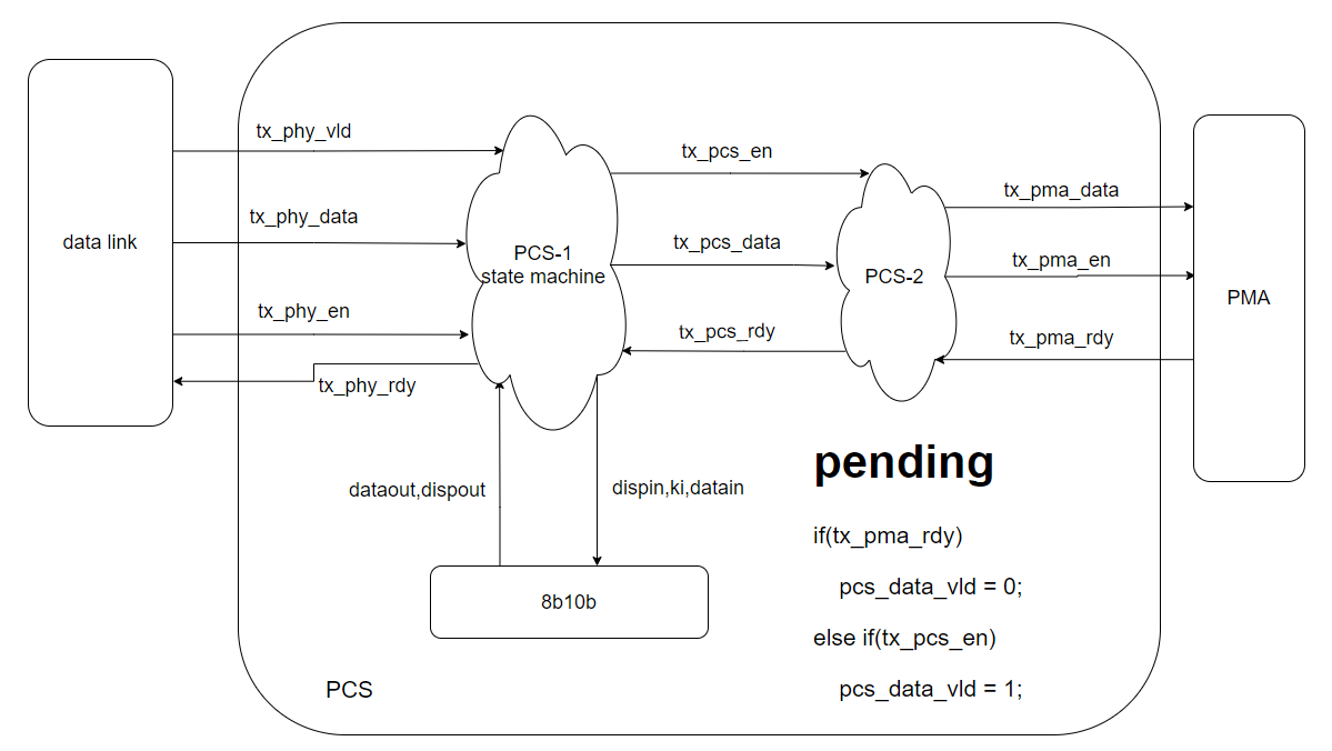
图7 PCS层结构图
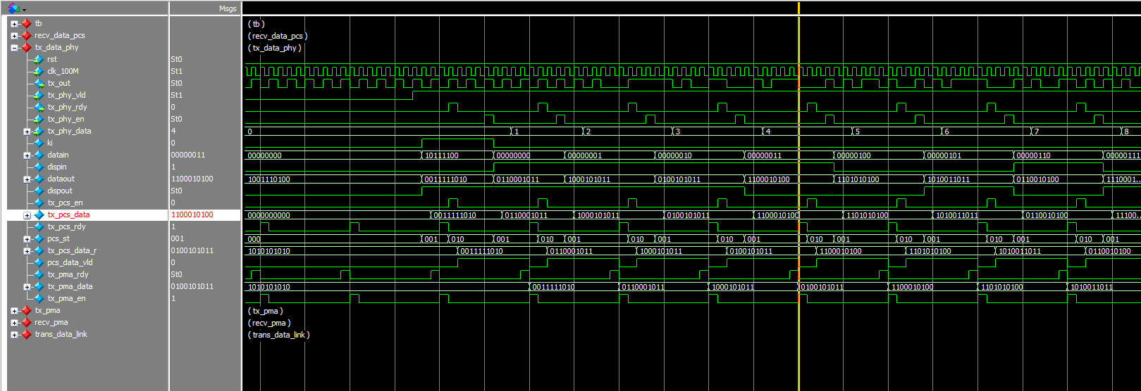
图8 tx_data_phy.v(PCS)仿真波形1
图8中应着重分析与上层 data-link以及下层PMA 层的握手,同时结合本层的程序,研究如何插入K28.5.
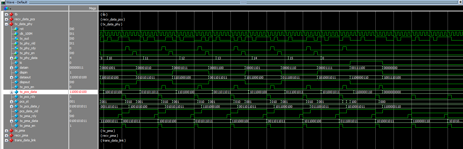
图9 tx_data_phy.v(PCS)仿真波形2
利用图9波形结合PCS层代码分析包结束部分的握手,以及如何插入K28.1控制字符。
5.发送端 PMA代码
本层主要实现并串转换,要注意与上层PCS子层的握手。
|
1 2 3 4 5 6 7 8 9 10 11 12 13 14 15 16 17 18 19 20 21 22 23 24 25 26 27 28 29 30 31 32 33 34 35 36 37 38 39 40 41 42 43 44 45 46 47 48 49 50 51 52 53 54 55 56 57 58 59 60 61 62 63 |
module tx_PMA ( input rst, input clk_100M, input tx_pma_en, input [ 9: 0 ] tx_pma_data, output reg tx_pma_rdy, output tx_out ); wire tx_in; reg [ 9: 0 ] tx_pma_data_r; reg [ 9: 0 ] tx_sft; reg [ 1: 0 ] tx_pma_st; reg [ 3: 0 ] sft_count; assign tx_in = tx_sft[ 9 ]; always@( posedge clk_100M or posedge rst ) if ( rst ) begin tx_sft <= 0; tx_pma_st <= 0; sft_count <= 0; tx_pma_data_r <= 0; tx_pma_rdy <= 0; end else begin if ( tx_pma_en ) begin tx_pma_data_r <= tx_pma_data; end tx_pma_rdy <= 0; if ( sft_count == 9 ) begin tx_pma_rdy <= 1'b1; tx_sft <= tx_pma_data_r; sft_count <= 0; end else begin sft_count <= sft_count + 1; tx_sft <= { tx_sft[ 8: 0 ], 1'b0 }; //for debug convenience purpose end end tx_PMD tx_PMD_inst ( .tx_in ( tx_in ), .tx_out( tx_out ) ); endmodule |
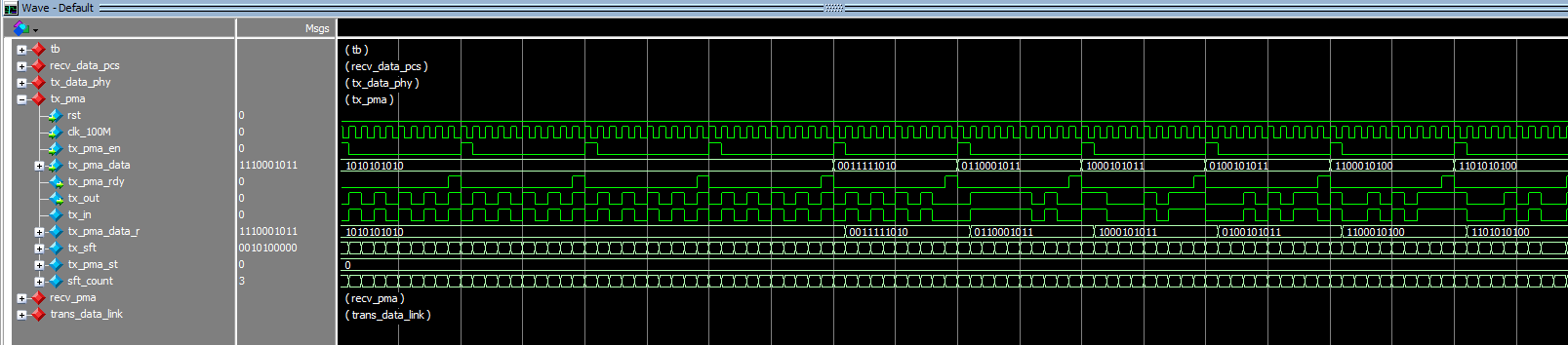
图10 tx_pma.v 波形
在图10中注意观察握手,以及上层如何调度IDLE和数据包的。
6. 发送端PMD代码
本层采用LVDS实现PMD(Physical Media Dependent),物理媒介可以是PCB板的差分线,或双绞线。
|
1 2 3 4 5 6 7 8 9 10 11 12 13 14 15 |
module tx_PMD ( input tx_in, output tx_out ); IO_TX IO_TX_INST ( .tx_in ( tx_in ), .tx_out ( tx_out ) ); endmodule |
以上6个部分的设计细节,由于过于繁琐,这里没有一一介绍,感兴趣的同学可以观看对应的视频。