
1.
根据下图给出的波形图,构建输出输出out的逻辑表达式。

|
1 2 3 4 5 6 7 8 9 |
module top_module ( input x, input y, output out ); // 使用assign语句实现 endmodule |
2.
对100-bit的输入向量in做以下操作:
- 判断in的每bit是否与左边相邻的bit都为1,即输出in[x] AND in[x+1] 的结果。因为in[99]没有左边相邻的bit,所以输出out_and为99-bit
- 判断in的每bit是否与右边相邻的bit任意为1,即输出in[x] OR in[x-1] 的结果,因为in[0]没有右边相邻的bit,所以输出out_or为99-bit
- 判断in的每bit是否与左边相邻的bit不相同,即输出in[x] XOR in[x-1] 的结果,定义in[99]左边的相邻bit为in[0],输出100-bit的out_xor
|
1 2 3 4 5 6 7 8 9 |
module top_module( input [99:0] in, output [98:0] out_and, output [99:1] out_or, output [99:0] out_xor ); //使用assign语句实现 endmodule |
对于接下来的问题,都是和时序电路相关,参考时序电路的基础Verilog 时钟的使用及触发器模型 。
3.
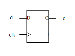
实现时序电路中常见的D触发器, 触发器应由 clk 的上升沿触发。
|
1 2 3 4 5 6 7 8 9 |
module top_module ( input clk, input d, output reg q ); // always @ (posedge clk)... endmodule |
4.
如果问题3中的d和q都是8-bit的向量,实现D 触发器,触发器应由 clk 的上升沿触发。
|
1 2 3 4 5 6 7 8 9 |
module top_module ( input clk, input [7:0] d, output reg [7:0] q ); // always @ (posedge clk)... endmodule |
5.
在问题4的基础上,添加一个高电平有效同步复位的 D 触发器。 触发器应由 clk 的上升沿触发。
|
1 2 3 4 5 6 7 8 |
module top_module ( input clk, input reset, //高电平有效同步复位 input [7:0] d, output reg [7:0] q ); endmodule |
6.
修改问题5中的触发条件为clk时钟的下降沿触发,并且在reset信号为高电平时,将q复位成0x39,而不是0。
|
1 2 3 4 5 6 7 8 |
module top_module ( input clk, input reset, //高电平有效同步复位 input [7:0] d, output reg [7:0] q ); endmodule |
7.
将问题5中的高电平有效同步复位的 D 触发器修改为高电平异步复位D触发器,触发器应由 clk 的上升沿触发。
|
1 2 3 4 5 6 7 8 |
module top_module ( input clk, input areset, //高电平有效异步复位 input [7:0] d, output reg [7:0] q ); endmodule |
8.
实现16-bit的D触发器,复位条件为低电平同步复位信号,注意这里添加了一个2-bit的byte_en:byte_en[0]控制q[7:0],byte_en[1]控制q[15:8]。触发器应由 clk 的上升沿触发。
|
1 2 3 4 5 6 7 8 9 10 11 |
module top_module ( input clk, input resetn, input [1:0] byteena, input [15:0] d, output reg [15:0] q ); endmodule |
参考代码:
[content_control]
[/content_control]
9.
实现以下电路,触发器应由 clk 的上升沿触发。

|
1 2 3 4 5 6 7 |
module top_module ( input clk, input in, output reg q ); endmodule |
10.
实现以下电路,触发器应由 clk 的上升沿触发。
|
1 2 3 4 5 6 7 8 |
module top_module ( input clk, input x, output z ); endmodule |
11.
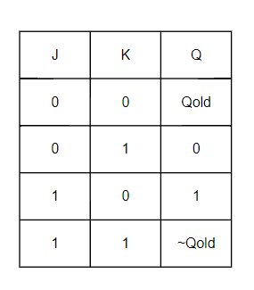
使用D触发器构建J-K触发器,注意Qold是Q在时钟上升沿到来之前的值,触发器应由 clk 的上升沿触发。
|
1 2 3 4 5 6 7 8 |
module top_module ( input clk, input j, input k, output Q); endmodule |
12.
检测输入8-bit向量in的每一bit何时从一个时钟周期的 0 变为下一个时钟周期的 1(上升沿检测)。下图特意列出了in[1] 和 pedge[1] 波形来说明。pedge是输出的8-bit向量。注意pedge对每个上升沿只维持了一个时钟周期。触发器应由 clk 的上升沿触发。
|
1 2 3 4 5 6 7 8 |
module top_module ( input clk, input [7:0] in, output [7:0] pedge ); endmodule |
参考代码:
[content_control]
[/content_control]
13.
在问题12的基础上,将检查上升沿的输出8-bit向量pedge换成检查任意边沿(上升沿或是下降沿)的8-bit向量anyedge,如下图所示。触发器应由 clk 的上升沿触发。
|
1 2 3 4 5 6 7 |
module top_module ( input clk, input [7:0] in, output [7:0] anyedge ); endmodule |
14.
检测输入32-bit向量in的每一bit何时从一个时钟周期的 1 变为下一个时钟周期的 0(下降沿检测)。如果没有高电平同步复位信号reset,对应的输出向量out会一直挂起,如下图所示。触发器应由 clk 的上升沿触发。
|
1 2 3 4 5 6 7 8 |
module top_module ( input clk, input reset, input [31:0] in, output [31:0] out ); endmodule |
参考代码:
[content_control]
[/content_control]
15.
双边沿触发器在Verilog中不存在相应的模型,不过可以通过巧妙的使用单边沿触发器实现。双边沿触发器的波形图如下所示:

|
1 2 3 4 5 6 7 8 9 |
module top_module ( input clk, input d, output q ); endmodule |
参考代码:
[content_control]
[/content_control]
对应视频: