
1.
模块例化,将下列模块sub_mod在顶层模块top_module例化。注意将sub_mod的输入连接top_module的输入,sub_mod的输出连接top_module的输出。
sub_mod模块如下:
|
1 2 3 4 5 6 7 8 |
module sub_mod( input in, output out ); // ... endmodule |
完善下列代码:
|
1 2 3 4 5 6 7 8 |
module top_module ( input a, output out ); //在这里例化sub_mod endmodule |
2.
通过信号对应位置例化模块。将下列模块sub_mod在顶层模块top_module例化。
sub_mod模块如下:
|
1 2 3 4 5 6 7 8 9 10 11 |
module sub_mod( input in1, input in2, input in3, output out ); // ... endmodule |
完善下列代码:
|
1 2 3 4 5 6 7 8 9 10 |
module top_module ( input a, input b, input c, output out ); //在这里例化sub_mod endmodule |
3.
通过信号名例化模块。将下列模块sub_mod在顶层模块top_module例化。
sub_mod模块如下:
|
1 2 3 4 5 6 7 8 9 10 11 |
module sub_mod( input in1, input in2, input in3, output out ); // ... endmodule |
完善下列代码:
|
1 2 3 4 5 6 7 8 9 10 |
module top_module ( input a, input b, input c, output out ); //在这里例化sub_mod endmodule |
4.
如果子模块sub_mod是一个d-flip flop,在顶层模块top_module例化4个移位寄存器,并将串行输出。
sub_mod模块如下:
|
1 2 3 4 5 6 7 8 9 10 |
module sub_mod( input clk, input d, output q ); // ... endmodule |
完善下列代码:
|
1 2 3 4 5 6 7 8 9 10 11 12 |
module top_module ( input clk, input d, output q ); wire q0,q1,q2; //在这里例化sub_mod endmodule |
上题中实现的是4位d-ff 串行输出,如果是100位,应该怎么做呢?
5.
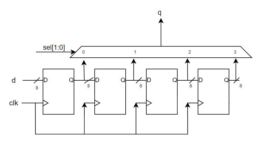
在问题4的基础上,将输入,输出端扩展成8-bit向量。并在顶层模块使用片选来选择输出,如下图所示:
sub_mod模块如下:
|
1 2 3 4 5 6 7 8 9 10 |
module sub_mod( input clk, input [7:0] d, output [7:0] q ); // ... endmodule |
完善下列代码:
|
1 2 3 4 5 6 7 8 9 10 11 12 13 |
module top_module ( input clk, input [7;0] d, input [1:0] sel, output [7:0] q ); wire [7:0] q0,q1,q2; //在这里例化sub_mod endmodule |
问题6~问题10可以参考文章Verilog 全加(减)器及累加器设计
6.
用简单逻辑门或Verilog语法实现1-bit全加器(参考文章提高数字系统设计性能–数字设计与Verilog 设计技巧一 算法)
|
1 2 3 4 5 6 7 8 9 10 11 12 13 |
module fadd ( input ci, input a, input b, output sum, output co ); //使用assign语句实现 endmodule |
7.
实现16-bit全加器(可以使用问题6中的1-bit全加器模块实现):
|
1 2 3 4 5 6 7 8 9 10 11 12 13 |
module fadd_16 ( input ci, input [15:0] a, input [15:0] b, output [15:0] sum, output co ); //在这里例化fadd endmodule |
8.
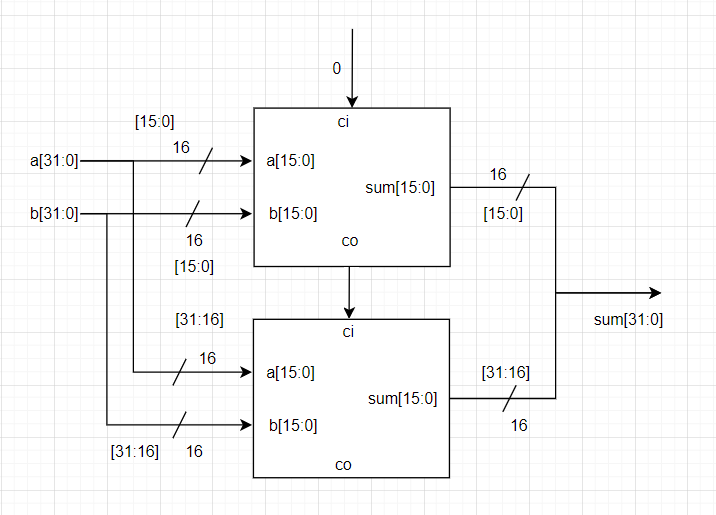
将问题7中的fadd_16 按照下图的连接方式在顶层模块进行例化:
完善下列代码:
|
1 2 3 4 5 6 7 8 9 10 11 |
module top_module ( input [31:0] a, input [31:0] b, output [31:0] sum ); //在这里例化16_adder endmodule |
9.
在问题8中可以看到计算sum[31:16]的fadd_16的ci需要计算sum[15:0]的fadd_16的co。注意上述算法的缺点是加法器的进位延迟可能相当慢,要等到第一级fadd_16完成后才能开始计算第二级fadd_16。 可以改进成进位选择加法器,如下图所示。 第一级加法器和以前一样,但是复制第二级加法器,一个假设进位=0,一个假设进位=1,然后使用一个快速的2-1 MUX来选择哪个结果是正确的。

完善下列代码:
|
1 2 3 4 5 6 7 8 9 10 11 |
module top_module ( input [31:0] a, input [31:0] b, output [31:0] sum ); //在这里例化16_adder endmodule |
10.
在问题7的基础上实现32位全加器全减器(根据信号sub来控制输出a + b或是a – b, sub ==0 ,加法; sub == 1 ,减法)。注意:全减器采用补码的方式实现,2进制补码对变量取反加一。
全减器仿真结果应该如下所示:

完善以下代码:
|
1 2 3 4 5 6 7 8 9 10 11 12 |
`timescale 1ns / 1ps module fsub_32 ( input [31:0] a, input [31:0] b, input sub, output [31:0] sum, ); endmodule |
提供的仿真文件如下:
|
1 2 3 4 5 6 7 8 9 10 11 12 13 14 15 16 17 18 19 20 21 22 23 24 25 26 27 28 29 30 31 32 33 34 35 36 37 38 39 40 41 42 43 44 45 46 47 48 49 50 51 52 53 54 55 56 57 58 |
`timescale 1ns / 1ps module TB(); wire [31:0] sum; reg [31:0] a; reg [31:0] b; reg sub = 0; initial begin #5; a = 0; b = 0; sub = 0; #5; a = 1; b = 0; sub = 0; #5; a = 2; b = 0; sub = 0; #5; a = 2; b = 1; sub = 1; #5; a = 2; b = 2; sub = 1; #5; a = 32'hffff; b = 1; sub = 0; #5; a = 32'h1_0000; b = 1; sub = 1; #5; a = 32'hffff_ffff; b = 32'hffff_ffff; sub = 0; end fsub_32 fsub_32_inst( .a(a), .b(b), .sub(sub), .sum(sum) ); endmodule |
对应视频: